
Microscopy Infrastructure for Semiconductor & Electronics Innovation
Semiconductor development increasingly depends on resolving smaller, more three-dimensional, and tightly integrated structures. Logic, memory, power electronics, MEMS, quantum devices, and advanced packaging require measurements that connect nanoscale structure with function, reliability, and failure.
TEM, STEM, SEM, FIB/SEM, and X-ray microscopy provide complementary views. Hummingbird Scientific develops the specimen environments, positioning systems, microfabricated devices, controls, and integration layers that connect them into practical experimental workflows.

Why advanced microscopy matters to the semiconductor industry
SEM supports device localization, critical-dimension measurement, surface and cross-section inspection, defect review, and failure analysis. FIB/SEM workflows expose buried structures and prepare site-specific lamellae for higher-resolution analysis. TEM and STEM reveal interfaces, crystal defects, diffusion pathways, strain, chemistry, electric fields, and atomic-scale structural changes that can determine device performance. X-ray microscopy and tomography add non-destructive three-dimensional information across larger volumes, including buried features, packaging structures, interconnects, and subsurface defects.
These techniques are increasingly used together. A region may be located in SEM, prepared by FIB, analyzed in TEM or 4D-STEM, revisited during heating or biasing, and correlated with X-ray or electrical measurements. The challenge is not only resolution. It is maintaining location, orientation, environmental history, electrical context, and data traceability across the workflow.
Hummingbird addresses these experimental layers through deterministic positioning, in situ specimen environments, microfabricated devices, controls, and open integration with the wider microscope and laboratory environment.
Infrastructure for advanced semiconductor microscopy
Advanced semiconductor microscopy requires more than imaging resolution. Repeatable positioning, controlled specimen environments, engineered sample interfaces, and connected experiment data help laboratories relate device structure to electrical behavior, processing history, reliability, and failure.
Deterministic positioning for repeatable semiconductor microscopy
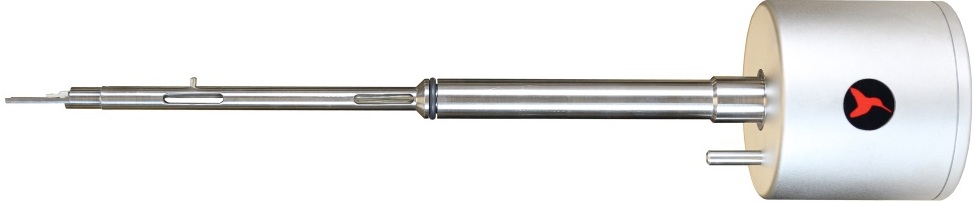
Hummingbird’s Precision TEM Stage is being developed for the next generation of microscope automation and semiconductor metrology. Conventional goniometers can make it difficult to return to a precise coordinate, preserve a region of interest through tilt, or execute repeatable multi-position measurements.
Closed-loop, deterministic motion can support region-of-interest return, automated defect review, tomography, 4D-STEM, diffraction mapping, correlative workflows, and repeated measurements of the same device structure. Preserving stage coordinates as part of the experiment record can help connect device layout, lamella position, structural measurements, electrical response, and later re-analysis.
In situ electrical, thermal, and environmental characterization
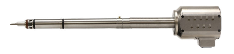
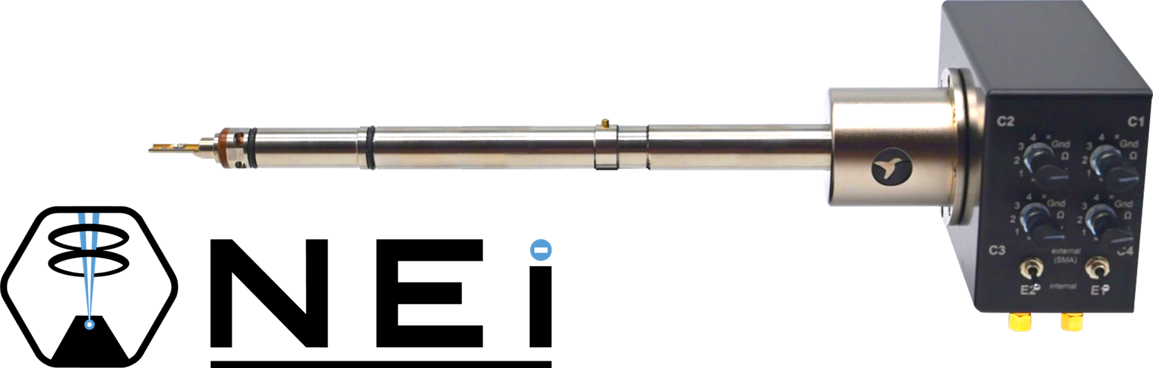
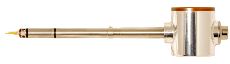
Device behavior cannot always be understood from a static image. Hummingbird systems support electrical biasing, MEMS heating and biasing, EBIC, cryogenic biasing and heating, gas and liquid environments, optical stimulation, nanomanipulation, air-free transfer, and tomography.
These tools allow researchers to observe switching, diffusion, phase transformation, electromigration, contact behavior, degradation, electrochemical processes, thermal stability, and field-driven changes while viewing the structure directly. Hummingbird’s broad portfolio allows laboratories to select the specimen environment that matches the device problem and connect the applied conditions and timing with the resulting microscopy data.
Microfabricated devices and custom sample interfaces
Semiconductor experiments frequently require electrode geometries, heater layouts, windows, carriers, contact patterns, or sample interfaces that are not available as standard consumables. Hummingbird’s in-house microfabrication capability supports MEMS heating chips, electrical and electrochemical devices, liquid and gas cells, window chips, X-ray devices, magnetizing devices, and custom designs for research and OEM programs.
Because microfabrication is connected to holder engineering, precision manufacturing, calibration, controls, and microscope testing, Hummingbird can develop the sample interface as part of the complete experimental system rather than treating the chip as an isolated component.
Open integration for semiconductor data and automation
Semiconductor microscopy produces more than images. It produces coordinates, tilt states, electrical conditions, temperature history, detector settings, microscope metadata, device identifiers, process context, and analysis outputs.
Hummingbird Connect™ supports defined and project-specific connections between Hummingbird hardware and OEM microscope workflows. Colibri Platform™ provides an open approach to structured experiment records and data handoff across OEM software, Python workflows, open-source analysis, institutional systems, LIMS, and future AI environments.
The microscope operating environment remains central. Hummingbird connects the physical experiment and its context without requiring the laboratory to replace the acquisition, analysis, or data-management tools it already trusts.
Why Hummingbird for semiconductor and electronics microscopy
Hummingbird brings together precision stage development, in situ specimen environments, EBIC, microfabricated devices, electronics, controls, open data integration, custom engineering, in-house manufacturing, calibration, and real TEM validation. These capabilities remain connected throughout development, allowing products and custom systems to be evaluated as complete microscope-integrated experiments.
For semiconductor companies, research institutes, microscope manufacturers, and metrology partners, Hummingbird can support standard products, application-specific modifications, custom devices, OEM integration, licensed technology, and joint development of new microscopy infrastructure.
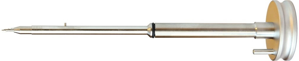
Hummingbird products for semiconductors and electronics


Bring your semiconductor experiment together
Build a semiconductor microscopy workflow around your device, your microscope, and your data environment. Talk with Hummingbird about deterministic stage positioning, in situ electrical testing, custom microfabricated devices, OEM integration, and advanced metrology development.