Print or download this brochure
To download a pdf on your tablet or mobile device, you can select the share option after selecting the button above.
View the full product page

›

NEI Two-Channel STEM EBIC System

Operando heating, biasing under environmental conditions

Electronic Characterization Inside the TEM

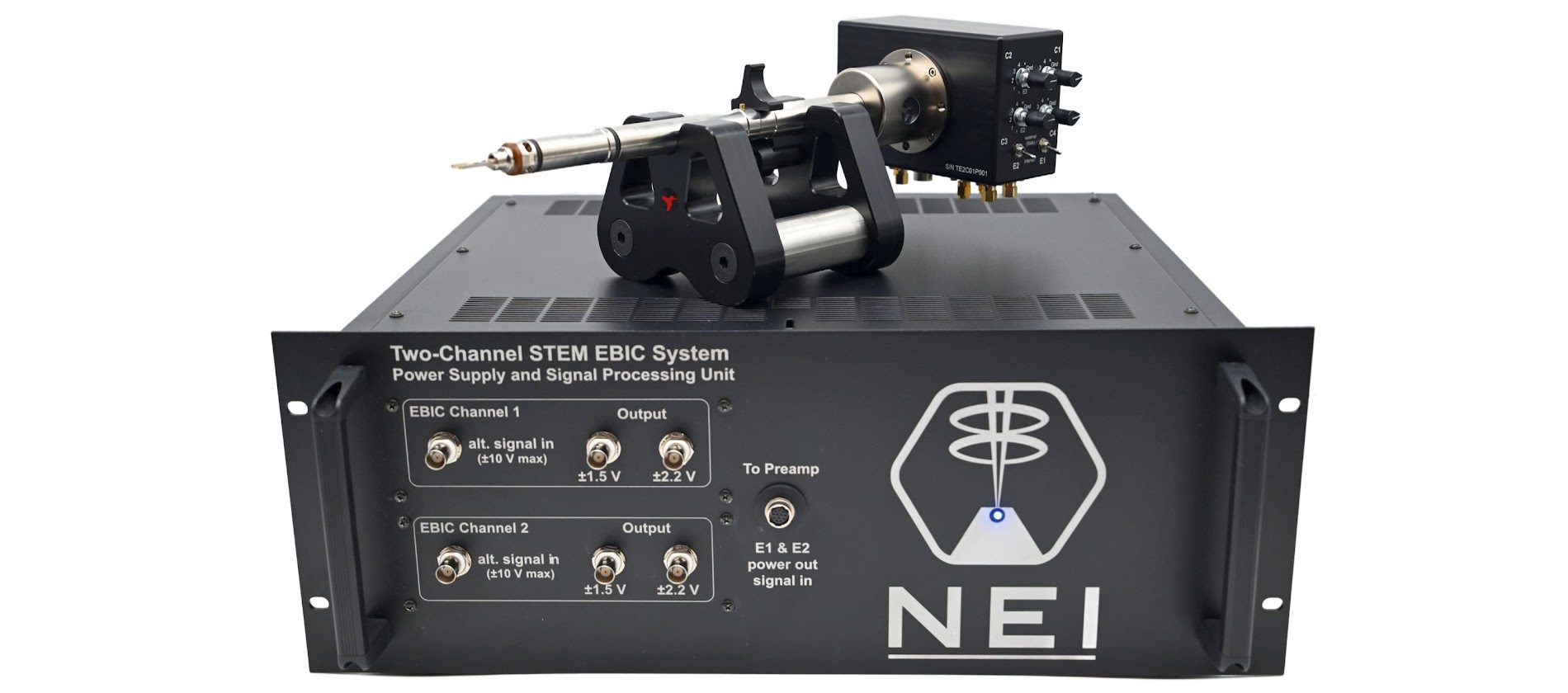
The NEI Two-Channel STEM EBIC System is a co-developed system from Hummingbird Scientific and NanoElectronic Imaging (NEI) that measures Electron Beam-Induced Current (EBIC) during TEM and STEM experiments. Combining a dedicated TEM holder, low-noise current measurement electronics, and compatible sample substrates, it simultaneously acquires Electron Beam-Induced Current (EBIC), Secondary Electron Electron Beam-Induced Current (SEEBIC), TEM/STEM imaging, Energy-Dispersive X-ray Spectroscopy (EDS), and Electron Energy Loss Spectroscopy (EELS) datasets for correlative electronic, structural, and chemical analysis.

‍

Accelerating Semiconductor and Functional Materials Research

Correlate conductivity, charge transport, electric fields, polarization, charge accumulation, and current pathways with crystal structure and composition during a single experiment. Two independent EBIC channels distinguish complementary current signals while maintaining direct correlation with ADF, BF, EDS, and EELS. Optional integrated heating extends the workflow to temperature-dependent electronic characterization.

‍

Correlative Analysis of Electronic, Structural, and Chemical Properties

Conventional TEM and STEM reveal morphology, crystallography, and composition but do not directly measure electronic properties. Electron Beam-Induced Current (EBIC) complements these techniques by mapping beam-induced current in electrically contacted samples. Correlate electronic, structural, and chemical information from the same nanoscale region to better understand device performance, material response, and failure mechanisms in semiconductor devices, functional materials, and nanoelectronic systems.

Technical Specs
???? series Single-tilt
???? series Double-tilt
Imaging method
TEM, STEM, EBIC, SEEBIC
2 on holder
EBIC biasing channels
2 on holder
TEM, STEM, EBIC, SEEBIC
Sample substrates
FIB Lift-out chips, patterned heating and biasing substrates, wet-transfer substrates
Tilt Range
Up to ± 45° depending on objective pole
Up to ± 20° (alpha and beta) depending on objective pole
Beta-tilt accuracy
N/A
<0.01 degree
Biasing Contacts
9 contacts
9 contacts
Contact Type
Direct Chip Contact
Direct Chip Contact
Heating Temperature
>1000 °C
>1000 °C
Temperature Stability
100+ hours
100+ hours
Temperature Measurement
4-point resistance sensing
EELS / EDS Compatible
Yes (full temp range)
Instrument Type
TEM
TEM

Available For:

Key Features and Capabilities

Integrated Heating

Study temperature-dependent electronic behavior while maintaining correlative TEM/STEM characterization.

Compatible Sample Substrates

Support diverse sample preparation workflows using compatible EBIC substrates.

Correlative EBIC, TEM/STEM, EDS, and EELS

Relate electronic properties directly to crystal structure and composition during a single experiment.

Direct Chip Loading

Reduce setup time while maintaining reliable electrical contact for repeatable electronic characterization.

Two-Channel Electron Beam-Induced Current Measurement

Acquire independent Electron Beam-Induced Current (EBIC) and Secondary Electron Electron Beam-Induced Current (SEEBIC) signals for correlative electronic characterization.

Advanced Configuration Options