How can 2D materials and alloys be engineered from more easily fabricated metal films?
Michael Motala, Nicholas Glavin, and their colleagues at the Air Force Research Laboratory, UES Inc., Rice University, University of Pennsylvania, UNICAMP, University of Dayton, and University of Illinois- Urbana-Champaign published on their use of the Hummingbird Scientific in-situ MEMS heating + biasing TEM holder to heat sub-nanometer sequentially-layered metal heterostructures on sapphire and SiO2 substrates.
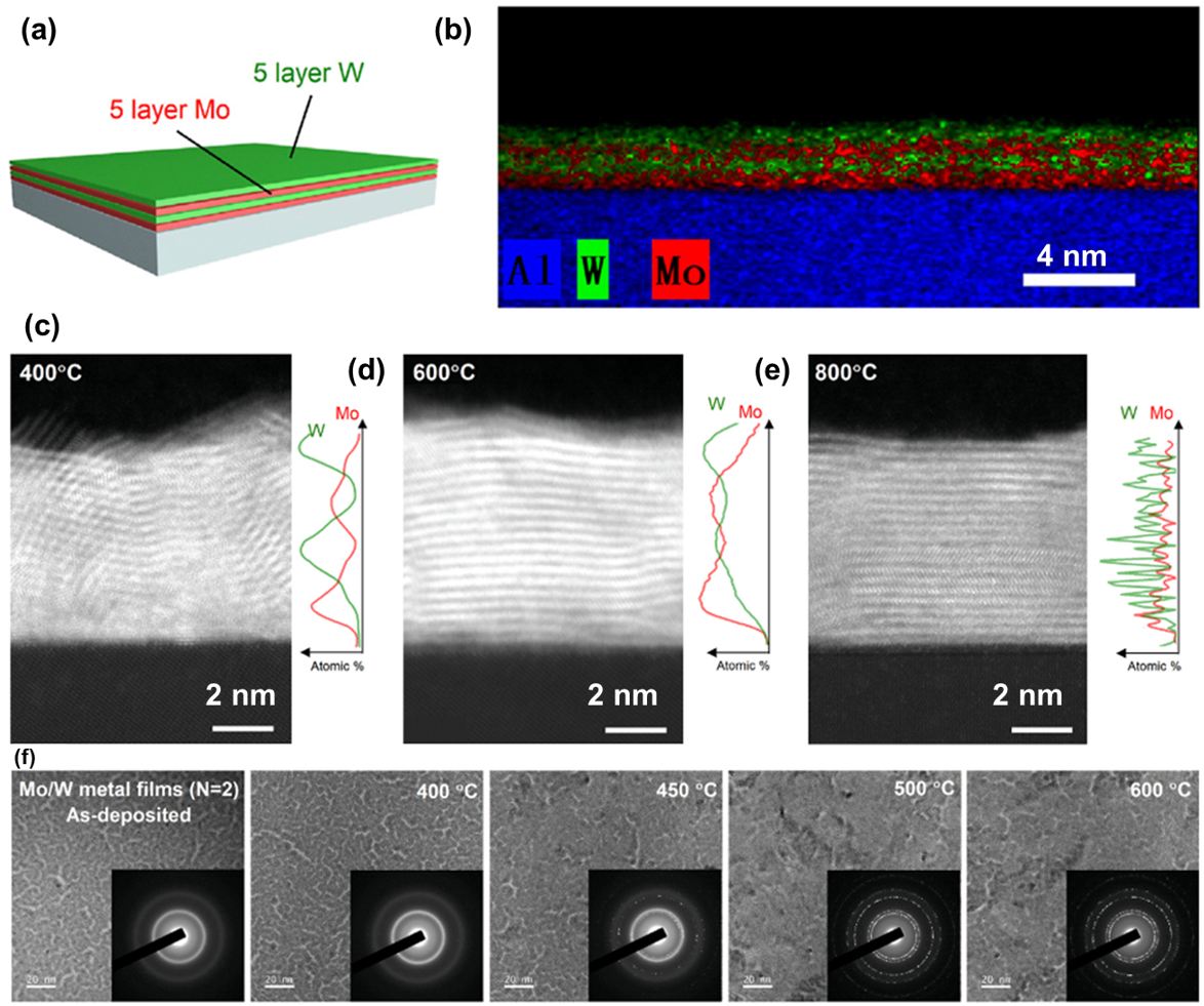
a) Schematic illustration of Mo/W superlattice. b) EDS map of Mo/W/Mo/W heterostructure. STEM and EDS spectra of sample annealed at c) 400 C, d) 600 C, and e) 800 C. f) In-situ TEM annealing of Mo/W metal films in vacuum, including bright field TEM images and SAED patterns. Copyright © 2024 Elsevier B.V.
Mo, W, and Mo/W layered superlattices were converted into MoSe2, WSe2 and MoSe2/WSe2 using H2Se annealing. Upon in-situ vacuum heating to various temperatures, the fabricated films converted into 2D van der Waals (vdW) superlattices, heterostructures, and alloys with novel bulk properties such as reduced bandgap, enhanced light-matter coupling, and increased catalytic performance. The Hummingbird heating + biasing TEM holder experiences minimal drift across the experimental temperature range, even at atomic resolution, enabling in-situ imaging of the atomic restructuring of metal films. The elegant synthesis procedure will facilitate rapid characterization and tailoring of novel materials for industrial applications.
M.J. Motala, X. Zhang, P. Kumar, E.F. Oliveira, A. Benton, P. Miesle, R. Rao, P.R. Stevenson, D. Moore, A. Alfieri, J. Lynch, D. Austin, S. Post, G. Gao, S.Mac, H. Zhu, Z. Wang, I. Petrov, E.A. Stach, W.J. Kennedy, S. Vangala, J.M. Tour, D.S. Galvao, D. Jariwala, C. Muratore, M. Snure, P.M. Ajayan, N.R. Glavin Materials Today Nano 22 100319 (2023) DOI: 10.1016/j.mtnano.2023.100319
Full PaperCopyright © 2024 Elsevier B.V.

.png)